Navigation Navigation |
|
| Characterization of nano-structure materials |
|
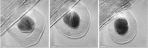
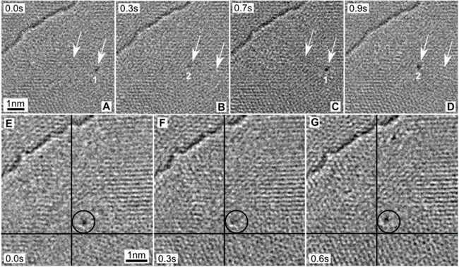
| Liquid-like pseudoelasticity of sub-10-nm crystalline silver particles |
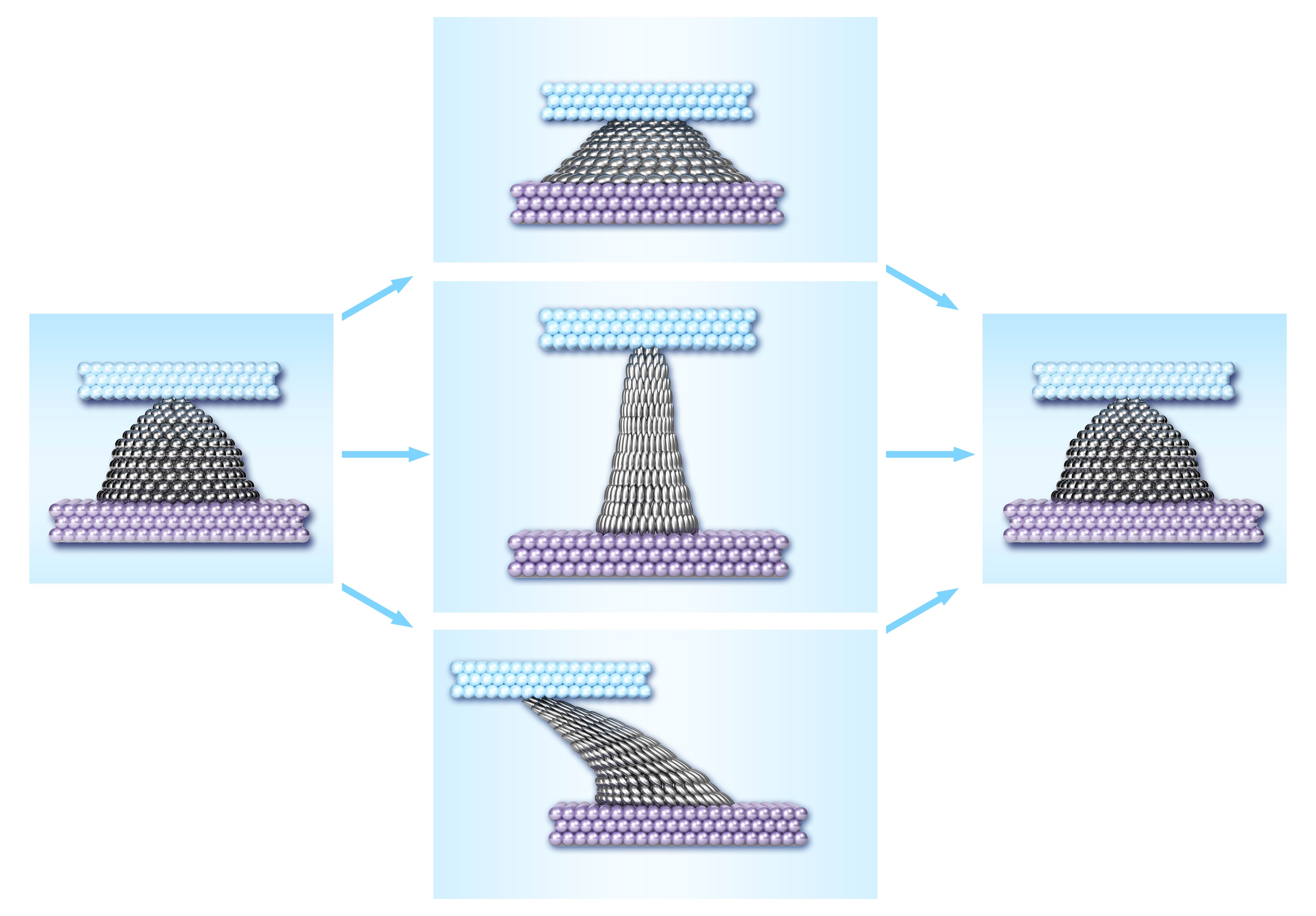
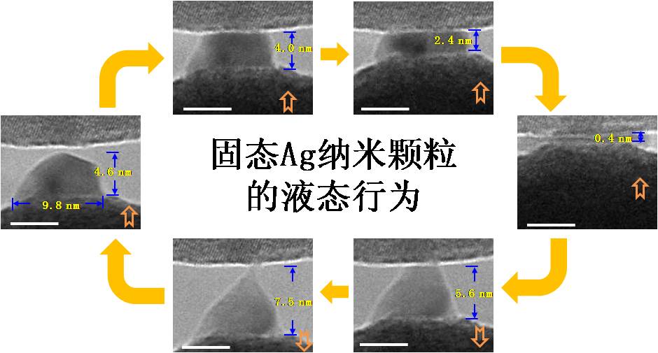
In nanotechnology, small-volume metals with large surface
area are used as electrodes, catalysts, interconnects and antennae.Their shape stability at room temperature has, however,been questioned. Using in situ high-resolution
transmission
electron microscopy, we find that Ag nanoparticles can be
deformed like a liquid droplet but remain highly crystalline
in the interior, with no sign of dislocation activity during
deformation. Surface-di�usion-mediated pseudoelastic deformation is evident at room temperature, which can be driven
by either an external force or capillary-energy minimization.
Atomistic simulations confirm that such highly unusual Coble
pseudoelasticity can indeed happen for sub-10-nm Ag particles at room temperature and at timescales from seconds
to months. |
|
Publication:Jun Sun, Longbing He,Yu Chieh Lo, Tao Xu,Hengchang Bi, Litao Sun,Ze Zhang*, Scott X.Mao and Ju Li*, "Liquid-like pseudoelasticity of sub-10-nm crystalline silver particles", Nature materials: 4105 doi:10.1038/NMAT 4105 (2014) |
| Hopping transport through defect-induced localized states in molybdenum disulphide |
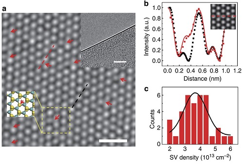
Molybdenum disulphide is a novel two-dimensional semiconductor with potential applications in electronic and optoelectronic devices. However, the nature of charge transport in back-gated devices still remains elusive as they show much lower mobility than theoretical
calculations and native n-type doping. Here we report a study of transport in few-layer molybdenum disulphide, together with transmission electron microscopy and density functional theory. We provide direct evidence that sulphur vacancies exist in molybdenum
disulphide, introducing localized donor states inside the bandgap. Under low carrier densities, the transport exhibits nearest-neighbour hopping at high temperatures and variable-range hopping at low temperatures, which can be well explained under Mott formalism.We suggest that the low-carrier-density transport is dominated by hopping via these localized gap states. Our study reveals the important role of short-range surface defects in tailoring the properties and device applications of molybdenum disulphide.
|
|
| Publication: Hao Qiu, Tao Xu, Zilu Wang, Wei Ren, Haiyan Nan, Zhenhua Ni, Qian Chen, Shijun Yuan, Feng Miao, Fengqi Song, Gen Long, Yi Shi, Litao Sun, Jinlan Wang & Xinran Wang "Hopping transport through defect-induced localized states in molybdenum disulphide", Nature Communications 4: 2642 doi:10.1038/ncomms3642 (2013) |
| Sub-nanometer molybdenum sulfide ribbons forming from a monolayer MoS2 sheet under electron irradiation. |
Developments in semiconductor technology are propelling the dimensions of devices down to 10 nm, but facing great challenges in manufacture at the sub-10 nm scale. Nanotechnology can fabricate nanoribbons from two-dimensional atomic crystals, such as graphene, with widths below the 10 nm threshold, but their geometries and properties have been hard to control at this scale. Here we find that robust ultrafine molybdenum-sulfide ribbons with a uniform width of 0.35 nm can be widely formed between holes created in a MoS2 sheet under electron irradiation. In situ high-resolution transmission electron microscope characterization, combined with first-principles calculations, identifies the sub-1 nm ribbon as a Mo5S4 crystal derived from MoS2, through a spontaneous phase transition. Further first-principles investigations show that the Mo5S4 ribbon has a band gap of 0.77 eV, a Young’s modulus of 300GPa and can demonstrate 9% tensile strain before fracture. The results show a novel top–down route for controllable fabrication of functional building blocks for sub-nanometre electronics. |
|
| Publication: X. F. Liu, T. Xu, X. Wu, Z. H. Zhang, J. Yu, H. Qiu, J. H. Hong, C. H. Jin, J. X. Li, X. R. Wang, L. T. Sun* & W. L. Guo “Top–down fabrication of sub-nanometre semiconducting nanoribbons derived from molybdenum disulfide sheets”, Nature Communications 4:1776 doi: 10.1038/ncomms2803 (2013) |
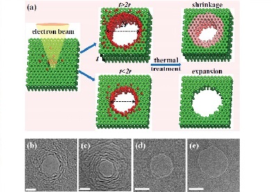
| Schematic of the fabrication and evolution processes of graphene nanopores. |
A sub-5 nm nanopore is necessary in single-molecule detections for biological and chemical applications because of the effect of its unique size and its strong interaction with various molecules. Focused electron beam-induced processing is the most widely used fabrication process, but the diameter of the nanopores fabricated by this approach cannot be precisely controlled because of the asynchronization of drilling and imaging under a single electron beam. We report a simple but reproducible technique for modulating the morphology of graphene nanopores by direct thermal heating without electron irradiation.
Graphene nanopores expand when pore diameter is larger than membrane thickness after heat treatment; otherwise, nanopore size shrinks. Such size-dependent evolutionary mechanism of nanopores is considered as thermal-induced migration of uncombined carbon atoms. The amount of carbon adatoms determines the extent of diameter change. This could provide an applicable strategy for nanopore fabrication.
|
|
| Publication: T. Xu, K. B. Yin, X. Xie, B. J. Wang, L. T. Sun*, “Size-Dependent Evolution of Graphene Nanopores Under Thermal Excitation”, Small, Volume 8, Issue 22, pages 3422–3426, November 19, 2012 |
| Fullerene as electrical hinge |
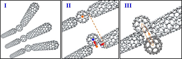
| The current study demonstrates that fullerenes with sizes between 1.9 nm and 3.3 nm serve as an efficient electrical hinges for interconnecting sub-5 nm carbon nanotubes (CNTs). Three modes of such “soft connections” were validated via transmission electron microscopy employing in-situ nano-manipulation and electrical transportation measurement. A high stability of the electrical connectivity caused by the forces acting between the fullerene and nanotubes was detected. Current densities as high as ~10^8 A/cm2, which almost reached the current carrier capability of CNTs, were observed within the nanocontact and a low contact resistivity (~10^-8Ωcm^2) was observed between the fullerene and nanotubes. |
|
| Three elemental contact modes
of the “electrical hinges” realized by connecting two CNTs via a fullerene. In contact mode I, the CNTs can change their relative angle by tilt and rotation. In contact mode II, the fullerene moves along the lateral direction. The orange and blue points indicate the position change of the fullerene. In contact mode III, the fullerene can rotate around the CNTs. In all modes, the connections are
mechanically “soft” and the electrical connectivity is preserved. Note the CNTs and fullerene could be multilayer structures, as the situation observed in the current experiments. |
|
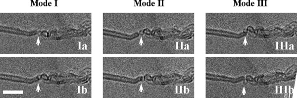
| TEM images of the three contact modes of the CNTs connected via a fullerene. The arrows show the different fullerene locations during electrical solicitation.In mode I (Ia and Ib), the CNT undergoes some displacement while the fullerene position remains almost unchanged. In mode II (IIa and IIb), the fullerene moves in the direction perpendicular to the image. In mode III (IIIa and IIIb), the fullerene moves from one side to the other. Bar=10 nm. |
|
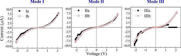
| The selected positively and negatively biased I–V curves of the CNT–fullerene–CNT contact. The labels correspond to the different contact geometries shown in Figure 2. |
| Publication: N. Wan, P. Perriat, L. T. Sun*, Q. A. Huang, J. Sun, and T. Xu, “Fullerene as electrical hinge” Applied Physics Letters 100, 193111-1-5(2012) |
| |
Investment casting of carbon tubular structures
|
Carbon nanotubes are promising candidates for NEMS devices such as in nano-electronics and nano-fluidics. However, several issues hinder their potential applications. First, the synthesis of carbon nanotubes is still uncontrollable. Conventional approaches like CVD are unable to fabricate carbon nanotubes with designed diameters and shapes. Second, construction of designed architectures with conventionally synthesized carbon nanotubes is difficult and complicated. There is still lack of a technique to freely manipulate a single carbon nanotube in nanometer precision. Besides, cutting & welding of synthesized carbon nanotubes are time- and energy- consuming. Third, welding of synthesized carbon nanotubes usually cause blocking of the conduits and this limit the application in nanofluidics.
To solve the above issues, we designed a novel method called “investment casting” to fabricate carbon nanotubes in precise control. With selected nanowires as templates, the carbon nanotubes could be fabricated with designed diameter, shape, wall thickness, and length. By construction of the template nanowires, carbon nanotube-based seamless architectures have been demonstrated. All these advantages can facilitate the application of carbon nanotubes for nanodevices. For more details of our method and results, please read the paper published on Carbon 50 (2012) 2845-2852. |
|
Publication:L. B. He, T. Xu, J. Sun, K. B. Yin, X. Xie, L. Ding, H. Xiu and L. T. Sun*, “Investment casting of carbon tubular structures”, Carbon 50, 2845-2854(2012) |
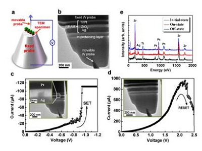
Real-Time Observation on Dynamic Growth/Dissolution of Conductive Filaments in Oxide-Electrolyte-Based ReRAM
|
|
| RS behavior and corresponding micro-structure changes during the in situ electrical test. |
Publications: "Real-Time Observation on Dynamic Growth/Dissolution of Conductive Filaments in Oxide-Electrolyte-Based ReRAM", Adv. Mater. 2012, 24, 1844–1849 |
| Migration and Trapping of metal atoms on strained graphene |
 |
PRL 105, 196102 (2010)
|
| |
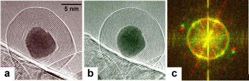
Elastic and Plastic Deformation of Single Nanometer-Sized crystals
|
|
Elastic deformation: Overlapping diffractograms obtained by Fourier transformation of the images in Fig.a displayed in red and Fig.b displayed in green. The distance of the spots from the center reflects the reciprocal spacings of the (111)-lattice fringes before and after irradiation. The lattice compression in Fig. b is reflected by the larger spacing between the green spots. |
|
Plastic deformation of metal crystal inside onion can be easily found by further irradiation |
|
| Extrusion of a gold crystal through a beam-induced hole (top left) from a spherical carbon shell under electron irradiation |
Publications:
1. L. T. Sun, F. Banhart, “The elastic deformation of nanometer-sized metal crystals in graphitic shell" Appl. Phys. Lett. 89, 263104 (2006)
2. Litao Sun, Arkady V. Krasheninnikov, Tommy Ahlgren,Kai Nordlund,and Florian Banhart "The plastic deformation of single nanometer-sized crystals" Physical Review Letters 101, 156101 (2008) See also commentary on article by S. Suresh and J. Li, Nature 456 (2008) 717 |
| |
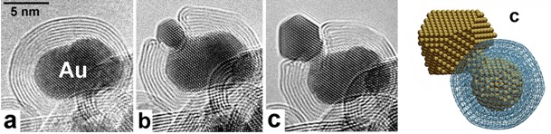
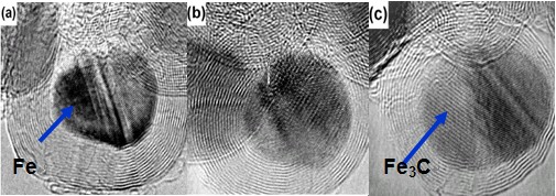
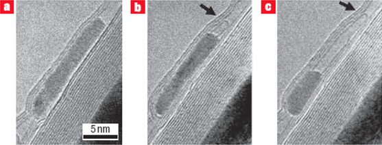
Carbon Onions and Nanotubes as Reaction Cells
|
|
Carbon onions encapsulating iron crystals of a few nanometers in size are subjected to electron irradiation in an electron microscope. A reaction between graphite and iron, leading to the formation of iron carbide (cementite) in the core of the clusters, is observed in situ. |
|
| The series of images shows the growth of a single-walled CNT (arrowed) from a cobalt crystal inside a host nanotube. (The host nanotube is sitting on a larger Co-filled nanotube.) The growth happens under electron irradiation at a specimen temperature of 600C, Image before growth. b, Image after 345 s of irradiation: a capped SWNT of nm in length has grown from the end face of the Co crystal. c, Image after 475 s; the SWNT has reached a length of 11 nm. |
Publications: 1. L. Sun, F. Banhart, “Graphitic Onions as Reaction Cells on the Nanoscale" Appl. Phys. Lett. 88, 193121(2006)
2. Julio A. Rodríguez-Manzo, Mauricio Terrones, Humberto Terrones, Litao Sun, Florian Banhart, Harold W. Kroto “In-situ nucleation of carbon nanotubes by the injection of carbon atoms into metal particles" Nature Nanotechnology 2, 307(2007)
3. Mauricio Terrones, Julio A. Rodríguez-Manzo, Humberto Terrones, Harold W. Kroto, Litao Sun, and Florian Banhart “Growing carbon nanotubes in a microscope" SPIE Newsroom: Nanotechnology DOI:10.1117/2.1200711.0934 |
| |
Irradiation Induced Nanofabrication and Phase Transformation
|
|
Ion irradiation induced transformation from carbon nanotubes to amorphous carbon nanowires and welding of carbon nanowires |
|
| Cutting of carbon nanotubes by electron irradiation |
|
| Single crystalline diamond nano-particles and nanorods synthesized by hydrogen plasma post-treatment of multiwalled carbon nanotubes |
Publications:
1. L. T. Sun, J. L. Gong, Z. Y. Zhu, D. Z. Zhu, S. X. He, Z. X. Wang "Nanocrystalline Diamond from Carbon Nanotubes" Appl. Phys. Lett. 84, 2901(2004)
2. L. T. Sun, Jinlong Gong, Dezhang Zhu, Zhiyuan Zhu, Suixia He “Diamond nanorods from carbon nanotubes" Advanced Materials 16, 1849 (2004) |
| |
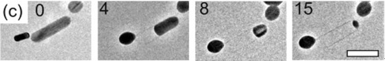
Thermal Stability of Nanomaterials
|
|
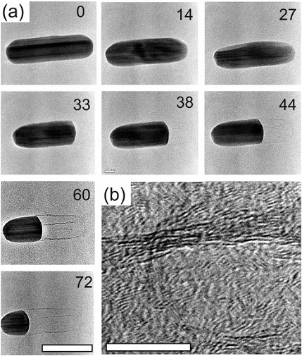
| (a) Sublimation of a silver nanorod at 885 K. Time as indicated (in minutes). The rod shrinks starting from the right leaving behind a shell structure. Solid part shows fringes indicating crystalline structure scale bars, 100 nm. (b) High-resolution image of the shell structure showing the typical appearance of graphitic filaments. Scale bar, 10 nm. (c) Details for a gold and a silver nanorod at the times indicated in the images (in min). Scale bars, 100 nm. |
Publications:
Yuriy Khalavka#, Christian Ohm#, Litao Sun#, Florian Banhart, Carsten Sönnichsen “Shape changes and sublimation of metal nanorods covered by thin surface layers” J. Phys. Chem. C 111, 12886(2007) # contributed equally and in alphabetical order |
| |
| |
|